SHRI SHIVAJI SCIENCE COLLEGE, AMRAVATI
DBT STAR COLLEGE PROJECT ACTIVITY
ACTIVITY REPORT

Industrial Visit to ECE India Energies Pvt. Ltd., Solar Panel Manufacturing Company
Activity Dates: 11/04/2025
Type of Activity: Field Studies
Organizing Department: Department of Physics
Program Coordinators: Dr. P.A. Fartode and Dr. S.S. Arsad
Head of the Department: Dr. P.A. Nagpure
External Collaborator (if any): No
Objectives:
- To provide students with practical exposure to the manufacturing process of solar panels.
- To connect classroom learning with real-world industrial practices.
- To understand the stages of solar cell and panel fabrication, including quality control measures.
- To inspire students towards career opportunities and further research in renewable energy technologies.
- To develop awareness of the economic and social impacts of solar energy in India’s clean energy future.
No of Beneficieries: 63
Classes Involved: B.Sc. I
Venue of the Activity: ECE India Energies Pvt. Ltd., Solar Panel Manufacturing Company, MIDC, Amravati
Activity Report:
1. Introduction
To bridge the gap between academic learning and real-world industrial practices, the Department of Physics, Shri Shivaji Science College, Amravati, organized a one-day industrial visit to ECE India Energies Pvt. Ltd., a leading solar panel manufacturing company, on 11th April 2025. This visit aimed at offering students a practical understanding of renewable energy technologies, especially photovoltaic (PV) systems, and exposing them to the actual processes involved in the manufacturing of solar panels.
The event was designed in alignment with the academic goals of providing experiential learning opportunities and promoting awareness of sustainable energy solutions among undergraduate students.
2. Participants
A total of 63 students from B.Sc. First Year, Semester II, enrolled under Physics Major/Minor subject groups, participated in the visit. They were accompanied by four faculty members and one non-teaching staff member, ensuring that the students were well-guided and disciplined throughout the visit. The accompanying team included:
Dr. S.S. Arsad
Dr. P.P. Khirade
Ms. S.M. Butte
Shri Vishwajeet Chavhan
One non-teaching staff member
The visit was coordinated and supervised by Dr. P.A. Nagpure and Dr. S.S. Arsad, who took responsibility for ensuring the visit’s smooth execution and educational relevance.
3. Pre-Visit Arrangements and Logistics
The students were instructed to assemble in Physics Laboratory II at 12:30 p.m., where attendance was duly recorded by Dr. P.A. Nagpure and Dr. S.S. Arsad. General instructions regarding discipline, dress code, safety protocols, and expected conduct during the visit were conveyed.
Two buses were arranged for transportation, and the group departed from the college premises around 1:00 p.m., reaching ECE India Energies Pvt. Ltd., located in the MIDC Area, Express Highway, Amravati-444607, by 2:00 p.m.
At the company entrance, each participant registered their name, contact number, arrival time, and signature. The management of ECE India strictly followed hygiene and safety protocols. Each student was provided with shoe covers and hair caps to ensure a clean and contaminant-free environment inside the production units.
To streamline the visit and ensure effective interaction, the students were divided into six batches, with approximately 12 students in each batch.
4. Company Overview
ECE India Energies Pvt. Ltd. is one of the fastest-growing solar energy companies in India. The company was founded in 2010 by Mr. Amit Arokar, who started his venture in a modest setup in Amravati. Today, it is ranked among the top ten PV module suppliers in India, with its products reaching domestic and international markets.
Key Highlights:
Direct Employment: 500+ individuals
Indirect Employment: Over 2,000 individuals
Target (by 2026): 1,000 direct employees
Solar Impact: Powering 35,000 homes, 2,000 industries, and 15,000 solar water pumps
Technological Achievements: Six patents related to PV efficiency, durability, and cost-effectiveness
ECE India stands as a beacon of innovation, sustainability, and community impact in the renewable energy sector. The company's vision includes empowering rural and urban communities through clean energy and contributing to India's commitment to reducing carbon emissions.
5. Detailed Explanation of Manufacturing Processes
The visit began with a guided walkthrough led by the company’s team manager and senior engineers, who explained each stage of solar panel production in detail. The key steps include:
1. Raw Material Sourcing and Preparation
Silicon Extraction: The process begins with the extraction of silicon from quartz sand. Students learned about the methods used to purify silicon and convert it into ingots.
Wafer Slicing: These ingots are sliced into thin wafers using high-precision cutting machines. The precision ensures minimal material waste and high efficiency in solar energy conversion.
2. Solar Cell Fabrication
Doping: Introduction of impurities like boron or phosphorus to create p-type or n-type semiconductors.
Texturing: Surface treatment to increase light absorption and minimize reflection losses.
Anti-reflective Coating: A specialized coating is applied to enhance photon capture.
Metal Contact Application: Formation of front and back contacts using fine silver or aluminum grids.
3. Panel Assembly
Stringing of Cells: Solar cells are electrically connected in series or parallel using soldered interconnections.
Encapsulation: Layers of EVA (ethylene-vinyl acetate) are used to encapsulate the cell string.
Lamination: The encapsulated structure is laminated under high temperature and vacuum to protect from moisture and physical damage.
Framing: Aluminum frames are fitted for structural support.
Junction Box Attachment: Diodes and wires are housed in a junction box fixed on the back side of the panel.
Sealing: Final sealing for water resistance and durability.
4. Testing and Quality Control
Visual Inspection: Manual checking for defects like cracks or alignment issues.
Electrical Testing: IV curve tracing, power output analysis, and fault diagnosis.
Quality Certification: Compliance with international standards like IEC, BIS, and MNRE.
Durability Testing: Exposure to stress conditions like heat, humidity, and mechanical load.
5. Packaging and Shipping
Solar panels are then packed in shockproof containers, labeled, and dispatched to warehouses or exported based on the demand.
6. Additional Demonstrations and Interactions
The visit included hands-on observation and demonstrations of several critical and advanced processes. These included:
LASER Cutting: High-precision LASER machines were used to cut modules accurately.
Silver Stripping: Students observed how unwanted silver from the contact lines was removed using chemical and physical methods.
Framing Techniques: Various machines for fitting aluminum frames and ensuring uniform insulation were demonstrated.
Logo Marking and Barcoding: Techniques used to imprint logos, barcodes, and traceability marks.
Fault Detection and Troubleshooting: Engineers showed how automated systems identify faulty cells and modules, and how these are separated for rework or disposal.
Performance Testing: Panels were tested under standard sunlight simulation conditions using flash testers.
7. Corporate Presentation
A video presentation was arranged in the conference room. It covered:
The company’s vision and mission
Growth timeline from 2010 to 2025
Environmental and social responsibilities
Participation in national clean energy initiatives
Scope for internships, industrial training, and project-based learning
Scholarship and stipend programs for undergraduate and postgraduate students
The session concluded with a Q&A round, where students asked insightful questions about panel degradation, cost economics, and innovations in energy storage.
8. Learning Outcomes
The visit proved highly beneficial in achieving the intended learning objectives. Key takeaways for the students included:
Firsthand experience of a real-world manufacturing ecosystem
Clarity on the structure and function of solar panels
Understanding the importance of cleanliness and precision in manufacturing
Exposure to modern engineering techniques like LASER cutting, lamination, and robotic testing
Insights into career prospects and internships in the solar industry
Recognition of India’s progress in the renewable energy sector
9. Conclusion
The industrial visit to ECE India Energies Pvt. Ltd. was an enriching experience for the students and faculty alike. It provided a unique opportunity to connect textbook knowledge with industry practices. The Department of Physics expresses its gratitude to the management and staff of ECE India for their hospitality, openness to education, and commitment to knowledge sharing.
The department also appreciates the discipline, enthusiasm, and curiosity shown by the students, and acknowledges the efforts of the accompanying faculty and staff in making the visit a success.
The visit stands as a testimony to the Department’s commitment to providing holistic, application-based education that inspires young minds to think innovatively and act responsibly toward a sustainable future.
Conclusion:
The visit concluded at around 5:00 p.m. with the group returning to the college.
The industrial visit to ECE India Energies Pvt. Ltd. was an eye-opening experience for the students. It provided hands-on insights into the solar panel manufacturing process, emphasized the importance of renewable energy, and highlighted the company’s commitment to quality, innovation, and sustainability. Students were inspired to consider research opportunities and internships in the solar energy sector.
A vote of thanks was extended to the company representatives for their warm hospitality, valuable guidance, and informative sessions.
Outcomes:
- Students gained a comprehensive understanding of the solar panel production process, from raw material extraction to final product shipment.
- Increased interest in pursuing internships and careers in the solar energy industry.
- Improved appreciation of quality control and testing procedures in industrial settings.
- Encouraged students to explore research opportunities and innovations in photovoltaic technology.
- Enhanced awareness of the importance of renewable energy in India’s energy transition.
Photos:
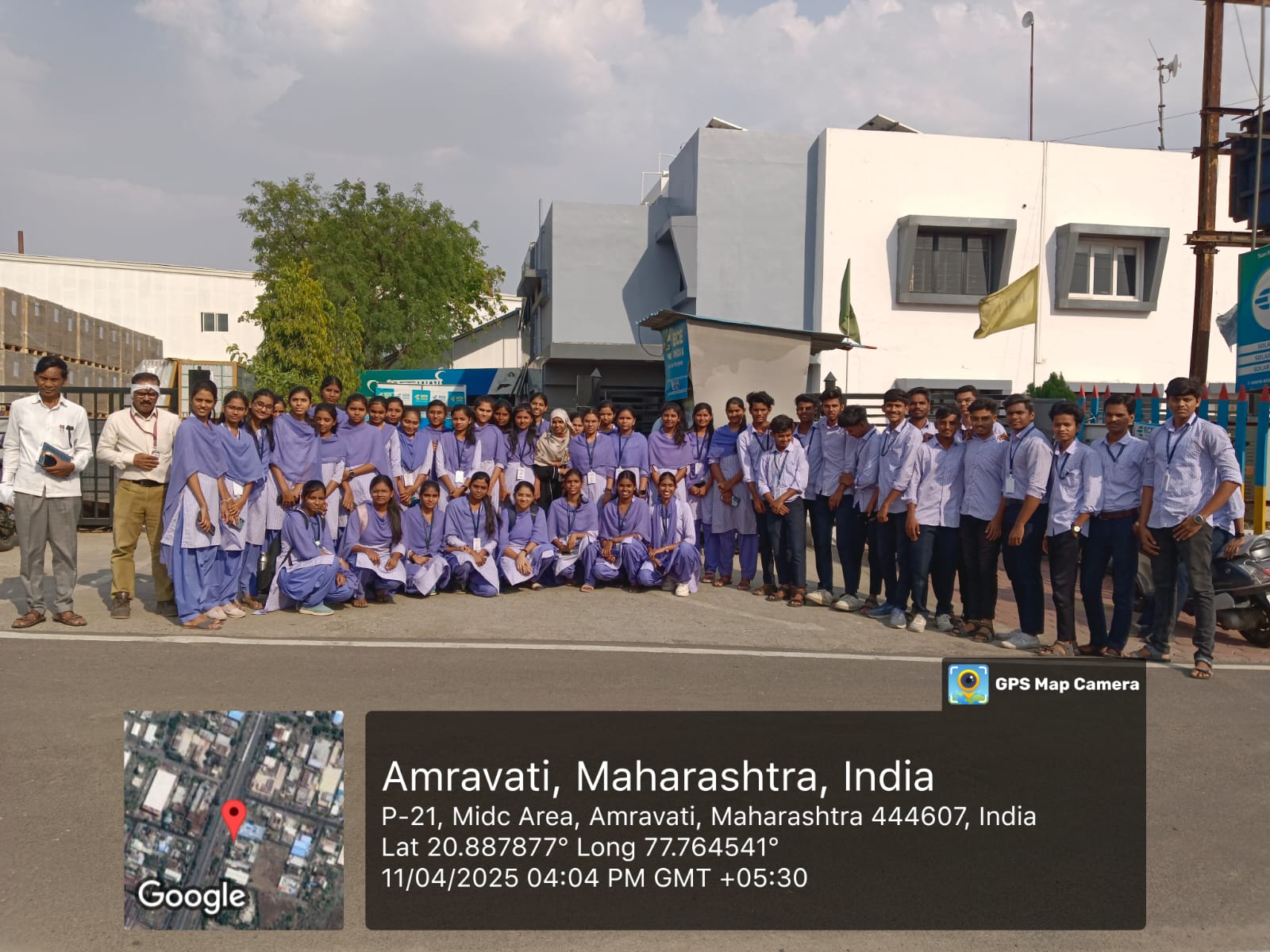 Students at ECE India Energies Pvt. Ltd., Solar Panel Manufacturing Company, MIDC, Amravati |  Industrial Visit ECE India Energies Pvt. Ltd., Solar Panel Manufacturing Company, MIDC, Amravati |
 Industrial Visit ECE India Energies Pvt. Ltd., Solar Panel Manufacturing Company, MIDC, Amravati |  Industrial Visit ECE India Energies Pvt. Ltd., Solar Panel Manufacturing Company, MIDC, Amravati |
 Industrial Visit ECE India Energies Pvt. Ltd., Solar Panel Manufacturing Company, MIDC, Amravati |  Students at ECE India Energies Pvt. Ltd., Solar Panel Manufacturing Company, MIDC, Amravati |
Attendance Sheet:
 Sheet |
 Sheet |
 Sheet |